

Usually we think of defects – structural imperfections – as “bad”, as something that diminishes the performance of a material, making it less perfect. However, in certain nanomaterials, such as carbon nanotubes, defects can be “good” and actually enable previously impossible functionalities. Controlling the number and type of such defects is crucial for their performance and potential applications.
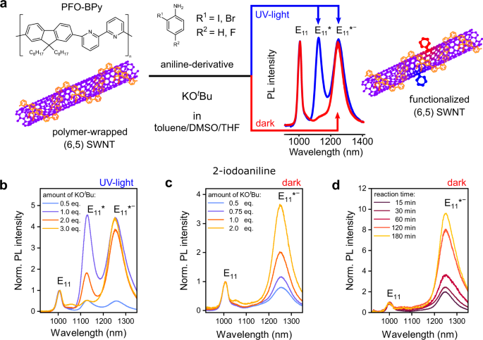
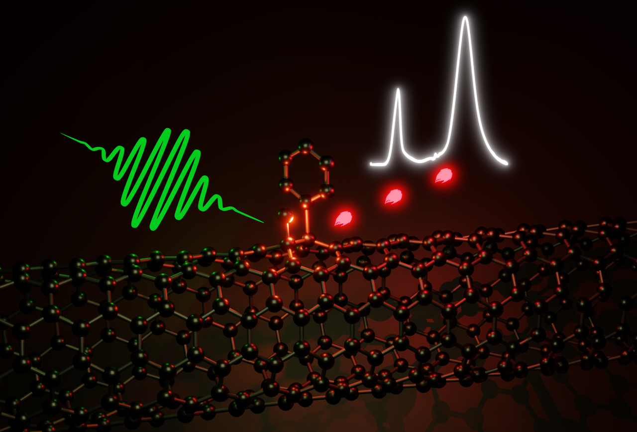
Carbon nanotubes are rolled-up sheets of graphene, that is, sp2-hybridized carbon atoms in a hexagonal lattice. These hollow tubes are about one nanometer in diameter and up to several micrometers long. They are excellent for charge transport and can emit light in the near-infrared, which is important for telecommunication and bioimaging. Through chemical reactions, a few sp2 carbon atoms of the nanotube lattice can be turned into sp3 carbon, which changes the local electronic structure and creates defect states that localize excitons. These so-called sp3-defects emit light even further in the near-infrared and increase the overall brightness. Because of the low symmetry of most carbon nanotubes, the precise position of the introduced sp3 carbon atoms determines the optical properties of the defects (e.g., the emission wavelength and the fluorescence lifetime). Unfortunately, so far there was very little control over what defects were formed.
We have found a new functionalization method to selectively create only one specific type of defect, which is even “better” than those that were previously accessible. By changing the reaction scheme from a radical to a base-mediated nucleophilic addition, the resulting defects emit light even further in the near-infrared and have much longer fluorescence lifetimes. As excitons are funneled to these defects the emission became much brighter compared to the pristine nanotubes. Due to the deeper optical traps of the achieved defects, even high-purity single-photon emission at room-temperature became possible. Single-photon sources emit one photon at a time and are necessary for quantum cryptography, which would enable highly secure telecommunication.
The chemical differences between the defects are very subtle and the desired binding configuration is usually only formed in a minority of nanotubes. Being able to produce large numbers of nanotubes with a specific defect and with controlled defect densities opens the path toward fabricating optoelectronic devices with them and thus also electrically pumped single-photon sources for quantum cryptography. The new functionalization scheme is very simple. It can be carried out in a beaker on a bench top at room temperature. No special equipment is needed. The exploration of potential applications (e.g., electroluminescent devices) is now under way. Many chemical and photophysical aspects of these defects are still unknown. Nevertheless, the goal is clear: making even better defects.
These results, published in Nature Communication, are the latest outcome of the ERC Consolidator Grant project “Trions and sp3-Defects in Single-walled Carbon Nanotubes for Optoelectronics” (TRIFECTs, Grant No. 817494) at Heidelberg University, which is dedicated to understanding and engineering the electronic and optical properties of defects in carbon nanotubes. For this publication we also collaborated with scientists at the Ludwig Maximilian University of Munich who performed single-photon measurements.
To learn more about this work, please read our article "Synthetic control over the binding configuration of luminescent sp³-defects in single-walled carbon nanotubes" in Nature Communications: https://www.nature.com/articles/s41467-021-22307-9
More about the group and the project: https://www.pci.uni-heidelberg.de/apc/zaumseil/index.html


Please sign in or register for FREE
If you are a registered user on Research Communities by Springer Nature, please sign in