While nanocrystals appear as promising building blocks for low-cost optoelectronics, their performances are often limited by their conduction properties. In a nanocrystal array, transport occurs though hopping mechanism, leading to limited carrier diffusion length, in the 10 to 100 nm range. In the case of HgTe nanocrystals, Lan et al. [1] recently proposed that transport actually occurs between island of strongly coupled nanocrystals. In other word, partly delocalize states are formed within these islands and the bottleneck for conduction becomes the link between these islands. Based on this idea, it becomes of utmost interest to probe transport at the scale of a single island where transport can efficiently occur.
Designing such small device is nevertheless challenging. Targeted sizes, below 100 nm, makes fabrication incompatible with traditional optical lithography. Even using e-beam lithography, it is actually challenging to obtain such scales particularly with long aspect ratio electrodes. Here, we use a smart concept inspired from single electron transistor fabrication and proposed by Dayen et al. [2-3] A first electrode is fabricated using an optical lithography. During a second step, this first electrode is used as a shadow mask while performing a titled evaporation. It thus becomes possible to build a nanotrench, see figure 1a. This corresponds to electrodes spaced by 40 to 80 nm and expanding over 30 µm. Device size resolution is no longer set by the wavelength of the light used for the lithography but rather by device geometrical factor. As a result, sub-wavelength devices can be obtained from a simple two-step lithography procedure.
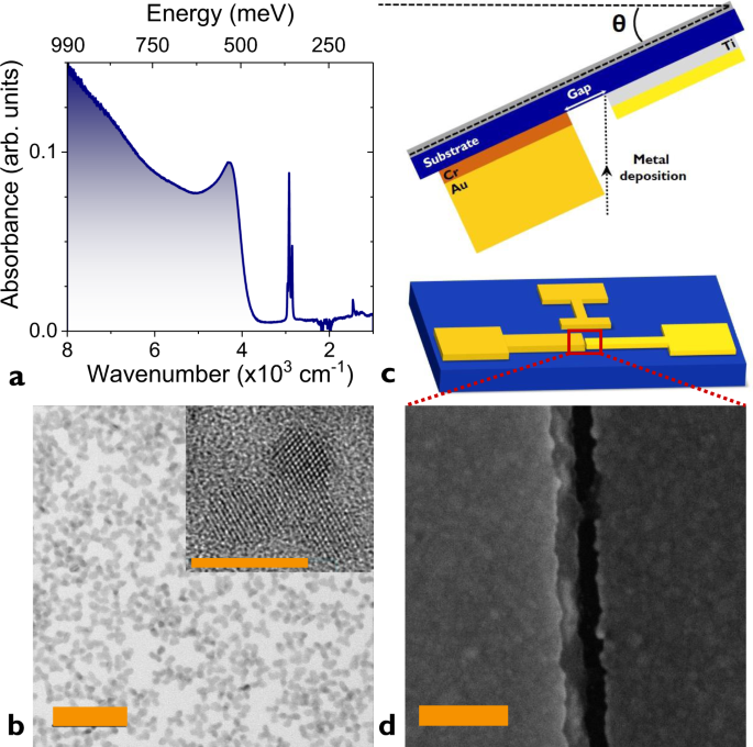
We observe that for such small devices the light responsivity of a thin film of HgTe nanocrystals exposed to infrared light is strongly enhanced compared to the same film deposited on µm-spaced electrodes. Because the device is small, gain is generated and quantum efficiency above 105 are achieved (corresponding to 105 electrons flowing per absorbed photons). This large gain enables large signal to noise ratio reaching 2x10¹² Jones at 200 K for a device with 2.5 µm cut-off wavelength, see figure 1b. This result over-performs the best photodiodes operating at the same wavelength. [4]

Figure 1 a Schematic of the nanotrench device: two electrodes spaced by a few 10s of nm and where the interelectrode gap is infilled by HgTe nanocrystals. b Detectivity (i.e. signal to noise ratio) for a film of HgTe nanocrystals as a function of the electrode spacing.
Many processes may explain such a responsivity enhancement. A first one may relate to charge dissociation resulting from the large applied electric field. However, the photoresponse shows no signature of such dissociation with no shift of the spectral response under bias application, see figure 2a. This observation is further supported by electronic structure simulations which predict only marginal change in the wavefunction overlap. A possible other mechanism at play may come from electromagnetic field enhancement, see figure 2b. We indeed observe a localization of the field within the nanogap and a polarized photoresponse (see figure 2c), but the effect is only expected to contribute for a factor 5 – 10 in the total enhancement. Finally using transport measurement, we confirm that transport is only driven by the part of the nanocrystal film located within the nanogap. It becomes possible to connect the photodetection performance to the change of transport mechanism in this part of the device. [4]

Figure 2 a Normalized photoresponse of the device for different applied bias. b Map of the absorption in TM mode (i.e. magnetic field along the trench) showing localization of the field within the nanogap. c Photoresponse along the two polarizations of light showing polarized response of the device.
This result is important since it contradicts a common thought in the field that only photodiodes enable highest performances. The next challenge will be to achieve a matrix of such electrodes.
Read our article in https://www.nature.com/articles/s41467-021-21959-x
References
[1] Quantum dot solids showing state-resolved band-like transport, X. Lan et al., Nature materials 19, 323 (2020)
[2] Nanotrench for nano and microparticle electrical interconnects, J-F. Dayen et al., Nanotechnology 21, 335303 (2010)
[3] Nanoplatelets bridging a nanotrench: a new architecture for photodetectors with increased sensitivity, E. Lhuillier et al., Nano letters 15, 1736 (2015)
[4] Infrared photoconduction at the diffusion length limit in HgTe nanocrystal arrays. Chu, A., et al. Nat Commun 12, 1794 (2021). https://doi.org/10.1038/s41467-021-21959-x


Please sign in or register for FREE
If you are a registered user on Research Communities by Springer Nature, please sign in