Achieving large-area carbon nanotube (CNT) arrays from random raw materials while preserving the surface cleanness and high alignment degree is of great importance to the development of ultra-robust CNT fibers and carbon-based integrated circuits. However, previous alignment techniques and efforts faced a series of drawback s, such as increased density of defects and impurities, barely satisfactory alignment, and short intrinsic lengths.
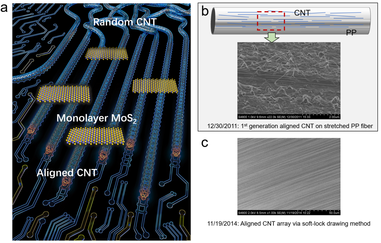
Our story of CNTs alignment originated from the year of 2011 when I was still a 2nd-year graduate student at Peking University (supervised by Prof. Anyuan Cao). My 1st trial happened at the end of 2011 (12/30/2012). At that time, I wrapped a piece of random CNT thin film on a polypropylene (PP) fiber to form a conductive and strong CNT-PP composite fiber. When a large strain was applied on the fiber, there occurred a plastic deformation of the PP matrix, and the randomly distributed CNTs on the surface were successfully aligned to some extent (Fig. 1b). At that moment, I realized that an external large mechanical force could effectively facilitate the uni-axial alignment of CNTs. However, the aligned CNTs could not be transferred to other substrates easily, such as SiO2/Si, so that further characterizations and device fabrication became very difficult. Later on, I tried different strategies to optimize the alignment technique. For example, I dispersed raw CNT powders into ethanol or water with the addition of surfactants. And one end of a living plant branch was inserted inside the CNTs dispersion solution. Assuming that the one-dimensional CNTs could be absorbed by the plant together with the water/ethanol, the CNTs were assumed to probably be aligned within the hollow vessel elements. This attempt also failed because of the difficulty of further characterization and transfer. The crucial step forward happened in early 2014, when I occasionally noticed the scratch of CNTs using the tip of tweezers could lead to the beautiful alignment of CNTs locally. This phenomenon inspired me to use a filter paper to replace the tweezer tip. As a result, large-area random CNTs were transformed into super-aligned CNT arrays (Fig. 1c). 
(a) Schematic illustration of using aligned CNTs as nm electrodes and interconnects in two-dimensional semiconductor transistors. (b) The 1st generation of alignment of CNTs on stretched PP fiber. (c) Alignment of CNTs following soft-lock drawing method.
In 2015, when I got my PhD degree and moved to the US for postdoc research, the alignment mechanism of CNTs was still unclear, and we could not figure out how to use these aligned CNTs in a unique way. It is very fortunate that I could continue to work on this project together with Dr. Yunfan Guo and Prof. Jing Kong at MIT since 2016. They provided extraordinary technical and original ideas and support to make the alignment mechanism clear and propose the idea of utilizing metallic CNTs bundles as the nanometer electrode and interconnect in two-dimensional (2D) semiconductor devices. In addition, with the help from Jiadi Zhu and Prof. Tomás Palacios, the idea of nanometer electrode was implemented and optimized successfully.
The discovery and optimization of our work takes more than one decade. This is a very special journey full of challenges and surprises. We feel very excited that we have developed this nondestructive and universal strategy to achieve ultra-clean CNT arrays with a very high degree of alignment. And a very unique “Gluttonous Snake” model was proposed to elucidate the alignment process, which could possibly lead to the microscopic manipulation of CNTs more precisely. In addition, we have found and come up with a unique application for individual metallic CNTs and bundles in electronic devices. Based on this work, we believe more opportunities could arise soon. For example, 1) this alignment strategy could be extended to semiconducting CNTs in a large area. 2) By further improving the control of the spatial location of all individual CNTs and the spacing between neighboring CNTs, the CNT electrodes could provide a way to make nanoscale contacts for 2D or 3D conventional semiconductors to the ultimate scaling of transistor contacts.
Read our paper in Nature Nanotechnology: https://www.nature.com/articles/s41565-021-01034-8


Please sign in or register for FREE
If you are a registered user on Research Communities by Springer Nature, please sign in