
Metal halide perovskite semiconductors possess outstanding characteristics for solar cells, light emitters, sensors, detectors and other optoelectronic applications. Low-dimensional and nanostructured motifs impart different functionality which can be exploited further. For example, two-dimensional perovskite structures have shown improved long-term operational device stability which is the main drawback preventing wide-spread commercialization of thin film perovskite photovoltaics. Zero-dimensional quantum dot perovskite structures exhibit strain-related phase stability and wider A-site composition tunability. Moreover, tunable surface ligand properties of colloidal quantum dot (QD) perovskites enable device architectures which differ from thin-film perovskites fabricated from solvated molecular precursors.
Heterostructures within photovoltaic devices offer control of the energy levels to enable better harvesting of photogenerated charge carriers. In solution-processed thin film perovskite photovoltaic devices, such a concept has is not widely explored primarily due to complications of the solvent from the second layer redissolving underlying layers.

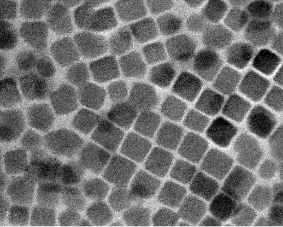
Fig. 1 Heterojunction structure of QD films. Schematic overview of layer-by-layer assembly showing a perovskite QD film composed of different layers of QDs. MeOAc treatment is carried out between the deposition of different QD layer to remove the native oleate ligands and to render the deposited QDs insoluble in the solvent.
In contrast, in perovskite QDs, the solvent works differently. Nonpolar solvents like hexane and octane suspend the perovskite QDs in solution by their bound organic ligands (oleate and oleylammonium, which have aliphatic chains with 18 carbons). Thus the solvents do not technically dissolve the precursors as in the case of thin films of ionic precursors solvated by polar aprotic solvents such as dimethylformamide or others. In layer-by-layer deposition of perovskite QD films shown schematically in Fig. 1, a layer of QDs is deposited from the colloidal solution onto a substrate and then ligands are chemically removed, enabling the resulting film to be insoluble to the solvent, thus enabling the ability to process the subsequent QD-layers without affecting the underlying film. In principle, subsequent layers can contain either the same QDs or QDs of different composition, size, morphology, etc. allowing for the overall composition of the perovskite film to be modulated in almost any desired order throughout the film thickness.

Fig. 2. Photovoltaic performance of solar cells. a, Cross-sectional STEM-HAADF image of devices with the structure of Glass/ITO/TiO2/Cs0.25FA0.75PbI3/CsPbI3/spiro-OMeTAD/MoOx/Al. The dashed line indicates roughly where the interface between the two types of QDs resides. b, SPO at 0.95 V of devices with different thickness ratio of Cs0.25FA0.75PbI3 layer to CsPbI3 layer in the perovskite QD absorber.
In this work, using layer-by-layer deposition of perovskite QDs, we structure the layers to create an internal heterojunction within the perovskite QD absorber layer (Fig. 2a) that improves charge separation at the internal interface leading to improved photocarrier harvesting. We show how the composition and position of the heterostructure can be optimized to boost the photovoltaic performance based on charge-carrier lifetimes and mobilities within each material to achieve a power conversion efficiency from stabilized power output up to 15.74%. This concept could be extended to QDs and other forms of absorber layers (thin films, 2D structures, or combinations therein). Furthermore, our approach should lead to a larger design-space which will impact a wider range of perovskite-based opto-electronic applications such as LEDs, transistor, (spintronic or quantum information processing, etc.).
More details can be found in our paper "High Efficiency Perovskite Quantum Dot Solar Cells with Charge Separating Heterostructure" published in Nature Communications: https://www.nature.com/articles/s41467-019-10856-z


Please sign in or register for FREE
If you are a registered user on Research Communities by Springer Nature, please sign in