Credit: poster image photographed by Felice Frankel.
https://www.nature.com/articles/s41563-018-0197-z
In this paper recently appeared in Nature Materials, we have created so-called colloidal electronics, or synthetic cells ("SynCells" for short) that physically resemble biological cells, but functionally analogous to an autonomous platform for modern microelectronic systems, all enabled and fabricated using low-dimensional materials (2-dimensional materials to be specific such graphene, molybdenum disulfide, and hexagonal boronitride). These are atomically thin, hexagonally arranged carbon atoms (in graphene), Mo and S atoms (in MoS2), or boron and nitrogen atoms (in hBN). By leveraging their superior electronic and mechanical properties (as well as chemical stability), we assembled them into lateral and vertical electronic circuits onto these extremely small (as small as the size of a human red blood cell), portable (with magnetic control of all modes of locomotion), autonomous platforms (or "SynCells") capable of next generation computing (untethered to an existing electronic grid) in its own local environments, on demand, with applications spanning environmental monitoring and biomedical sensing. Operationally, these "SynCells" could one day be injected into a human body for long-term, minimally-invasive medical diagnosis for accessing data such as micro-lesions that are not available using current diagnostic tools.
The materials science advance, introduced here for the first time, is a fabrication method of these SynCells which we have termed "autoperforation". This "automatic perforation" of essentially any 2-dimensional materials of interest provided a scalable alternative to conventional photolithography for assembling a whole class of materials into artificial, synthetic organelles with a stable colloid form-factor, representing one of the only ways available right now to produce stand-alone integrated microelectronics on a large scale that are functional off the chip (a large area supporting substrate such as a silicon wafer).

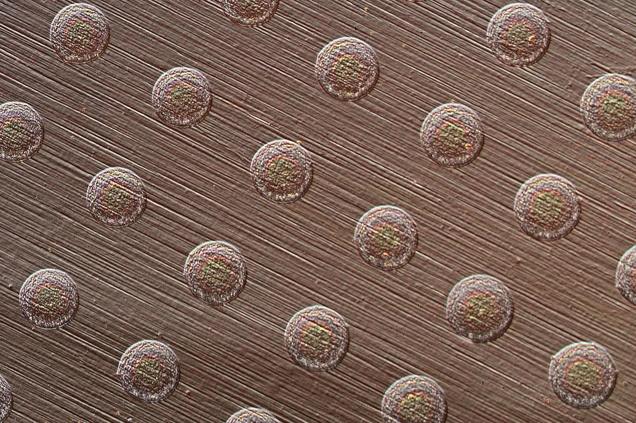
This was achieved using a controlled fracturing process. The fracturing of brittle materials, such as these 2-dimensional materials or others as common as a gorilla glass used in the iphone screen, are typically perceived to be stochastic, uncontrollable, and above all, undesired. But as it turns out, an imposed strain field within such brittle materials could actually guide crack growth, using something called the Griffith theory established 100 years ago within the mechanics field. The big advance for us here, is to show that such a theoretical construct can be extended downward to the nanoscale, as a practical means to engineer and fabricate micro-electronic devices via the controlled rupture of 2D materials with superb electronic and mechanical properties, attractive for next generation computing.

We do so by ink-jet printing arrays of composite micro-pillars (or micro-disks) out of plane, and sandwich them in between two independently addressable layers of 2D materials, thereby "programming in" a circular stress-strain field within the 2D atomic lattice, fostering a controlled crack nucleation and the subsequent propagation upon further perturbation, effectively "cutting" these 2D atomic "skins" tailored around the enveloped composite disks. This "self-assembly of material defect" strategy, introduced here as a nanofabrication technique, then form the basis for the creation and demonstration of various types of autonomous micro-electronic devices capable of different functions such as locomotion, detection, and memory storage. This general procedure of using controlled fracture as a production method, as we have shown in the manuscript, can be extended across many length scales, towards essentially any 2D materials of choice, in principle allowing future researchers to tailor these atomically-thin surfaces into any desired shape or form for applications in other disciplines.


Please sign in or register for FREE
If you are a registered user on Research Communities by Springer Nature, please sign in
Hi Albert, please consider including this content in the Flatchat channel too!
Regards
Silvia